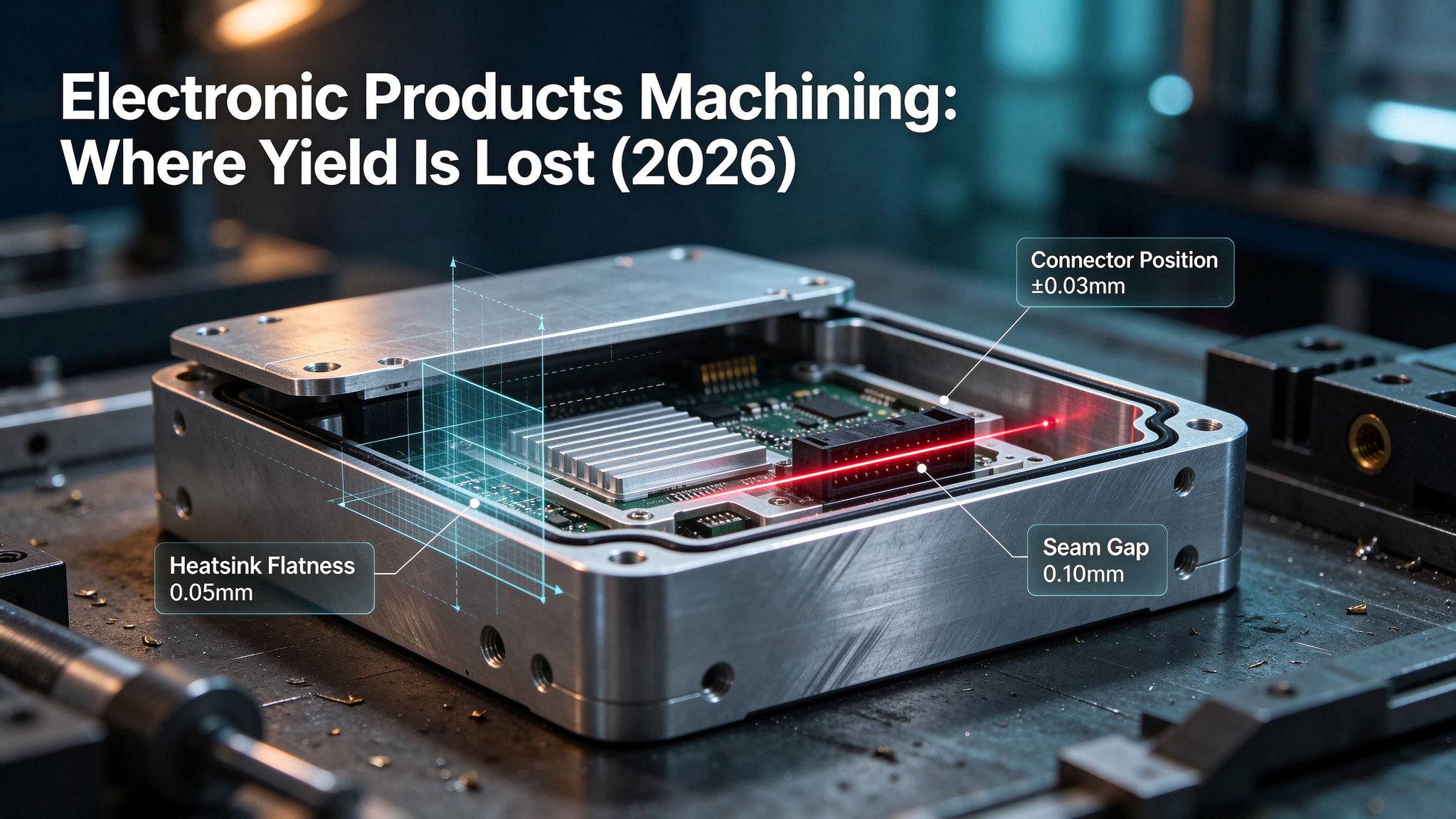
Electronic products machining is the mechanical half of electronics manufacturing — the enclosures, heatsinks, connector housings, shields and brackets that hold a PCB in place, keep it cool, and stop it radiating. When first-pass yield drops, the SMT line gets blamed. In most cases the cause is a machined dimension that was made exactly to print, and the print did not model the stack.
If you are already holding a yield problem and a drawing, send it to our engineering team — we will check the stack-up before you cut another batch.
Key Takeaways
- Most yield loss on electronic products starts in a machined dimension, not on the assembly line.
- Four tolerances decide it: connector hole position, heatsink flatness, enclosure seam gap, and shield contact depth.
- Worst-case stack-up overstates risk and statistical stack-up understates it. Neither is valid unless it matches how you measure.
- A 0.05 mm air gap under a heatsink costs roughly 3 K/W. Filling the same gap with thermal compound drops it to about 0.03 K/W.
- Seam gaps only matter relative to wavelength: at 2.4 GHz (125 mm), a 40 mm seam is 0.32λ and radiates.
Why Yield Problems Get Blamed on the Assembly Line
A typical pattern: a product runs at 98% first-pass yield through the prototype build, then settles at 91% in production. The reaction is to audit the SMT line, reflow profile, stencil and placement accuracy. Weeks later the actual cause turns out to be mechanical — a connector that needs 4 N of insertion force instead of 2 N, a heatsink that contacts only half its area, or a lid that will not sit flat because the gasket groove is 0.08 mm shallow.
Three things make this hard to see:
Machined parts are inspected against the drawing, not against the assembly. A part at the center of its tolerance band can still fail when combined with a PCB at the top of its band. Both are “in spec”. The failure belongs to the stack, and nobody owns the stack.
Mechanical failures look electrical. A connector that is 0.15 mm off center produces a marginal solder joint that passes AOI and fails in the field. A heatsink with a 0.1 mm bow produces a junction temperature 8 °C higher, which shows up as thermal throttling rather than a defect.
The measurement method is weaker than the tolerance. A ±0.02 mm callout verified with calipers on a 300 mm part is a ±0.1 mm callout in practice. The tolerance was never real.
The fix is not tighter tolerances everywhere — that multiplies cost for no yield gain. It is identifying the four dimensions that actually gate yield, specifying them in a way that can be measured, and controlling the stack around them.
The Four Machined Tolerances That Decide Yield
Across consumer electronics, telecom hardware, instruments and industrial control boards, the same four characteristics recur. They are worth more engineering attention than the other two hundred dimensions on the drawing combined.
| Characteristic | What it actually controls | Typical production spec | How it fails |
|---|---|---|---|
| Connector hole position | Insertion force, mating alignment, solder joint quality | ±0.03 mm true position across the connector group | Intermittent open circuit, rework, field returns |
| Heatsink base flatness | Thermal contact area and interface resistance | 0.05 mm over 50 mm (0.02 mm on premium parts) | Thermal throttling, derated performance, shortened life |
| Enclosure seam gap | EMI containment, gasket compression, ingress | 0.10–0.15 mm closed gap, groove depth ±0.05 mm | Radiated emissions failure at certification |
| Shield slot and contact depth | Ground continuity, shield seating | ±0.05 mm | EMC failure, intermittent ground, noise |
The rest of this article takes each one apart, with the numbers that make the failure predictable rather than mysterious.
Connector Pitch: The Cumulative Drift Nobody Models
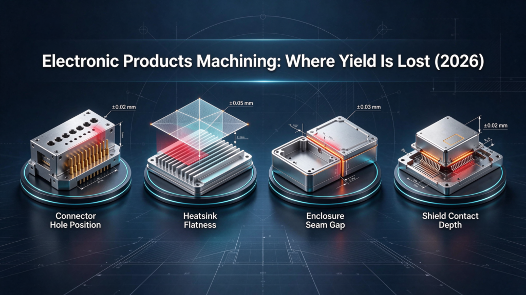
A 0.5 mm pitch connector with 40 pins spans 19.5 mm. Each hole is specified to ±0.03 mm true position, which sounds tight. It is tight — per hole. The problem is that insertion force depends on the relative position of the first hole and the last, across a 19.5 mm span, after the PCB has expanded and the connector has been soldered.
Two stack-up methods give very different answers:
| Method | Calculation | Result across 40 holes |
|---|---|---|
| Worst case (arithmetic) | 40 × 0.03 mm | ±1.20 mm — absurd, and nobody builds to it |
| Statistical (RSS) | 0.03 × √40 | ±0.19 mm — plausible, and closer to reality |
| Measured on a real batch | CMM, 30 parts, 40 holes each | typically ±0.06 mm at 3σ if machined in one setup |
The gap between ±0.19 mm (modelled) and ±0.06 mm (measured) is the entire argument for process capability over tolerance arithmetic. But the measured number only holds if all 40 holes are machined in one setup, from one datum, on one machine.
Move half the holes to a second operation and the number changes character. Re-fixturing introduces a fixture-to-part offset of 0.03–0.08 mm that is not random — it is a constant shift affecting every part in the batch. Statistical stack-up assumes randomness; a systematic offset is not random, and it does not average out.
Two rules follow:
- Machine all connector holes in a single setup. On a 3-axis machine this may mean a fixture that presents the part once; on 5-axis CNC machining it usually means no re-fixturing at all.
- Datum from the connector side, not the part edge. If the datum is a cast or extruded edge with its own ±0.15 mm tolerance, the connector inherits that error no matter how precisely the holes are drilled.
For through-hole connectors, add one more check: hole diameter tolerance and drill wear. A 0.1 mm oversize hole reduces insertion force but also reduces solder fillet strength — the joint passes inspection and fails under thermal cycling. Hole diameter should be specified ±0.02 mm with a defined reaming operation, not left to drill tolerance.
Heatsink Flatness: 0.05 mm Costs 3 K/W
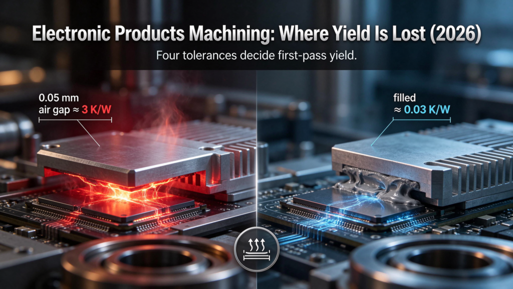
Flatness on a heatsink base is usually specified as an afterthought, because it looks like a cosmetic property. It is not. It is the dominant term in the thermal path when the interface is air or a thin compound.
The arithmetic is simple. Thermal resistance across a gap is:
R = t / (k × A)
For a 0.05 mm air gap (k = 0.026 W/mK) over a 600 mm² contact area (0.0006 m²):
R = 0.00005 / (0.026 × 0.0006) ≈ 3.2 K/W
At 10 W dissipation that is a 32 °C rise across a gap thinner than a human hair. Fill the same gap with a 3 W/mK thermal compound and the bulk resistance drops to about 0.03 K/W — a hundredfold improvement. Contact resistance at both interfaces typically doubles that again, so a realistic greased joint lands near 0.1–0.2 K/W. Still an order of magnitude better than air.
This is why heatsink flatness matters more than most engineers expect, and why it matters only when the interface is dry or poorly filled:
| Interface | Dominant resistance | What flatness buys you |
|---|---|---|
| Bare metal on metal, dry | Air gap, ~3 K/W | Everything. 0.05 → 0.02 mm roughly halves it |
| Thermal grease, 50 µm | Bond line + contact | Modest. Below 0.05 mm the return is small |
| Gap pad, 0.5 mm | Pad bulk | Almost nothing. The pad absorbs the gap |
| Phase-change / solder | Bond line | Nothing, but voiding becomes the risk |
Practical specification for machined heatsinks:
- Flatness: 0.05 mm over the contact footprint for standard parts; 0.02 mm where the design relies on dry contact or where the device dissipates more than 15 W.
- Surface roughness: Ra 0.8–1.6 µm. Smoother is not better — below Ra 0.4 µm, compound can pump out under thermal cycling and the joint degrades.
- Base thickness: enough to resist clamping load. A 3 mm base under four M3 screws at 1.5 Nm bows by 0.03–0.08 mm, which cancels the flatness you paid for.
- Method: face milling or fly cutting on a stable fixture, with the fin side supported. Machining a thin base in a vise will spring and produce a concave face.
One more failure mode worth naming: residual stress. Extruded 6061 bar stock carries internal stress. Machine 2 mm off one side and the part bows after it leaves the machine — flat when inspected, 0.1 mm bowed on the customer’s bench two days later. Symmetrical material removal, or a stress-relief anneal before finish machining, prevents it. If a supplier cannot explain how they handle this, they are not measuring flatness after stabilization.
For material options and their thermal conductivity, see our precision machining materials hub; for heatsink-specific alloys, aluminum CNC parts covers 6061, 6063 and 7075 with their trade-offs.
Enclosure Seams: Comparing Gap to Wavelength
An enclosure seam is an aperture. Apertures leak in proportion to their size relative to the wavelength of the field trying to escape. That makes “acceptable gap” a frequency-dependent number, not a fixed tolerance — and it is the single most common reason a product passes functional test and fails EMC.
Free-space wavelength is 300 mm at 1 GHz, 125 mm at 2.4 GHz and 60 mm at 5 GHz. The design rule that holds up in practice is to keep the longest dimension of any aperture below λ/20 at the highest frequency of concern:
| Frequency | Wavelength | λ/20 target | What that means for a seam |
|---|---|---|---|
| 1 GHz | 300 mm | 15 mm | A 40 mm seam is 0.13λ — leakage, but manageable with gasketing |
| 2.4 GHz | 125 mm | 6.25 mm | A 40 mm seam is 0.32λ — radiates efficiently, needs a gasket |
| 5 GHz | 60 mm | 3 mm | Almost any uninterrupted seam leaks; gasket pitch becomes critical |
At 2.4 GHz a 40 mm unbroken seam is about a third of a wavelength. That is an efficient slot antenna. No amount of shielding paint on the inside fixes it — the gap is the antenna, not the surface.
What this means for the machined part:
- Gasket groove depth tolerance is the critical dimension, not the gap itself. A groove specified 1.5 mm deep ±0.05 mm, with a 2.0 mm gasket, gives 25% compression — inside the useful 30–50% band only if the gasket is sized for the low end.
- Groove width should be +0.10/0 mm, so the gasket compresses rather than binds.
- Corner radii must match the gasket’s molded corner, or the seal lifts at the four corners and creates local apertures exactly where the seam is longest.
- Flatness of the mating faces matters as much as the gap: a 0.1 mm bow over 100 mm means the gasket is compressed at the ends and open in the middle.
Die-cast enclosures add two complications that machined enclosures avoid: draft angle (typically 1–2°) means the seam faces are never parallel, and parting-line flash leaves a 0.1–0.2 mm step that no gasket fully seals. Machined enclosures from billet have neither — which is why low-volume and high-frequency products usually start as machined parts even when the production intent is casting.
Shield Contact and Slot Depth

Board-level shields are mechanical parts doing an electrical job. Two dimensions decide whether they work:
Slot depth — the machined pocket that receives the shield frame. If it is 0.05 mm shallow, the can sits proud and the contact fingers do not compress; if 0.05 mm deep, the can bottoms out before the fingers engage. Either way the shield is present and not grounded, which reads as an EMC failure with no visible defect.
Contact finger pitch vs seam length — a shield with fingers every 2 mm behaves like a continuous wall at 2.4 GHz; one with fingers every 8 mm behaves like a series of slots. The machined pocket must position the frame so the fingers land on solid metal, not on a hole or a component.
Plating choice then decides how long that contact lasts. Tin plating is cheap and oxidizes; contact resistance can rise from 5 mΩ to 50 mΩ over a year in humid conditions. Nickel is stable at higher cost. Gold is stable and expensive. On a machined shield frame, specify the plating and the contact resistance limit together — “tin plated” alone is not a specification.
Stack-Up: Why Four ±0.05 mm Become ±0.35 mm
Here is a worked example from a typical handheld product: a machined base with a pocket for the PCB, a PCB of nominal 1.6 mm, a connector of nominal 3.0 mm, and a machined lid with its own pocket.
| Element | Nominal | Tolerance |
|---|---|---|
| Base pocket depth | 4.00 mm | ±0.05 mm |
| PCB thickness | 1.60 mm | ±0.10 mm |
| Connector height | 3.00 mm | ±0.15 mm |
| Lid pocket depth | 1.20 mm | ±0.05 mm |
| Closed gap | 0.40 mm | — |
Worst case: 0.05 + 0.10 + 0.15 + 0.05 = ±0.35 mm — the faces can interfere or open to 0.75 mm. Neither extreme is acceptable.
Statistical (RSS): √(0.05² + 0.10² + 0.15² + 0.05²) = √0.0375 ≈ ±0.19 mm. Better, but still marginal for a lid that has to compress a gasket by 30%.
The practical answer is usually not to tighten all four tolerances. It is to:
- Move the tolerance to the cheap part. Tighten the lid pocket to ±0.02 mm (one face, easy to control) and leave the PCB tolerance alone — you cannot change a purchased PCB anyway.
- Convert the gap into a controlled feature. Machine a step whose depth is set by the same setup as the mating face, so the error cancels rather than accumulates.
- Specify the assembly, not the parts. State “closed gap 0.10–0.15 mm with gasket compressed 30–50%” on the drawing. A supplier who understands the assembly will manage the stack; one who only reads individual dimensions will not.
Notice that the connector’s ±0.15 mm dominates. That single part contributes 64% of the variance and it is the one you cannot machine. Buying a connector with a tighter height tolerance, or selecting a different part, often does more for yield than tightening any machined feature.
Measuring What Actually Matters
A tolerance that cannot be verified is a suggestion. Before specifying ±0.03 mm, check what the shop can actually measure, and apply the 10:1 rule — gauge accuracy should be one tenth of the tolerance.
| Characteristic | Correct instrument | Sampling | What the report must show |
|---|---|---|---|
| Connector hole position | CMM with true-position evaluation, or vision system | 5 parts per lot, all holes | Position deviation per hole, Cp/Cpk |
| Heatsink flatness | Surface plate + indicator, or CMM plane fit | Every lot | Flatness value and measurement points |
| Gasket groove depth | Depth micrometer or CMM | 5 parts per lot | Depth, plus groove width |
| Seam gap, assembled | Feeler gauge on built unit, or CMM on both faces | First article + 3 per lot | Gap at four corners and mid-span |
| Shield slot depth | Depth gauge, CMM on first article | Every lot | Depth relative to frame datum |
Two practical notes. Calipers have ±0.03 mm accuracy and 0.02 mm resolution — they cannot verify a ±0.03 mm tolerance, yet they are used for it constantly. And a CMM report without the measurement uncertainty stated is only half a report; at ±0.03 mm tolerance, a 0.005 mm uncertainty already consumes 17% of the band.
Specifying for Yield, Not for the Drawing
Most drawings specify dimensions. The ones that produce high yield specify the relationship between dimensions. Six callouts do most of the work:
| Callout | What to write | Why |
|---|---|---|
| Datum scheme | Datum A on the connector face, B and C on two perpendicular edges of the same face | Stops the connector inheriting a cast edge’s tolerance |
| Position tolerance | True position, ⌀0.06 mm, referenced to A/B/C | Forces a functional gauge rather than a linear dimension |
| Flatness | 0.05 mm over the contact footprint, with the footprint bounded | Prevents applying flatness to the whole base |
| Surface texture | Ra 1.6 µm, lay direction perpendicular to coolant flow | Roughness without direction is unmeasurable in practice |
| Plating | Thickness range plus maximum contact resistance | “Tin plated” is not a spec |
| Assembly condition | Closed gap 0.10–0.15 mm, gasket 30–50% compression | Puts the stack on the drawing, where someone owns it |
The last one is the one almost nobody writes, and the one that prevents the most returns.
Materials and Finishes That Move the Numbers
Material choice changes the tolerances you can hold and the thermal numbers you calculated:
- 6061-T6 aluminum — 167 W/mK, machines cleanly, holds ±0.02 mm on a stable fixture. The default for machined heatsinks and enclosures.
- 6063 — higher conductivity (around 192 W/mK) and better anodize response, but softer and gummier to cut. Good for extruded profiles, less good for tight-tolerance pockets.
- ADC12 die-cast — roughly 92 W/mK. A die-cast enclosure conducts about half as well as a machined 6061 one, which is why casting conversions often need a bigger heatsink or a copper spreader.
- Copper and brass — copper for spreaders and high-flux paths, brass for connector shells and terminals. See brass CNC machining for the alloy trade-offs, including the leaded grades that fail RoHS.
- Engineering plastics — PC for flame-retardant housings, PC/ABS for cost, POM for mechanisms, PA for wear parts. Plastic CNC machining covers machining behavior, which differs sharply from metal: plastics move after cutting and need stress-relief passes.
Finishing matters twice. Anodize Type II adds 10–25 µm and moves dimensions by roughly half that outward, so critical features must be compensated before plating. Bead blasting changes surface texture and can close a 0.05 mm slot. And powder coat at 60–100 µm will destroy a connector alignment if applied after assembly. Our plastic finishing services page covers the full finishing chain, including the color-consistency controls that consumer electronics housing programs need. When the program sits between electronics and general consumer products – knobs, bezels, decorative hardware – the same cosmetic controls are covered on our consumer goods machining page.
The general principle: qualify the finish before you qualify the dimension. A part that is right before plating and wrong after it is not a right part.
Prototype to 500,000 Units
The mechanical approach changes with volume, and the thermal numbers change with it:
| Stage | Quantity | Process | What changes |
|---|---|---|---|
| Validation | 1–100 | CNC from billet, CNC milling and CNC turning | ±0.005 mm available; geometry is free to change |
| Pilot | 100–5,000 | CNC with dedicated fixtures | Setup time per part drops; flatness control improves |
| Bridge | 5,000–20,000 | CNC or soft tooling | Cost per part falls; inspection sampling replaces 100% check |
| Mass production | 20,000+ | Die casting or forging plus finish machining | Draft angles appear, thermal conductivity drops, tooling locks geometry |
Two warnings for anyone planning the casting conversion: die-cast surfaces cannot hold the same flatness as machined ones without a finishing cut, and the conductivity drop from 167 to 92 W/mK can invalidate a thermal design that was validated on machined prototypes. Plan the thermal margin for the production process, not the prototype process.
Sourcing Electronic Product Parts from China
The verification that matters is not the certificate, it is the measurement record. For electronic product parts specifically, ask for:
- First article inspection with true-position data, not just pass/fail.
- Material certificates matched to the heat number, plus plating thickness reports.
- Process capability for the four critical characteristics — Cpk ≥ 1.33, computed from at least 30 parts, not asserted.
- The fixture drawing. If a supplier cannot show how connector holes are located in one setup, the tolerance story is incomplete.
- A statement of what they will do when a dimension drifts — reaction plan, not reassurance.
A CNC machining factory that runs ISO 9001:2015 should produce all five without being asked twice. If you are comparing suppliers across regions, our CNC machining China page covers lead times, shipping terms and the practical differences in how drawings are interpreted.
Five Mistakes Buyers Make
1. Tolerancing every dimension to ±0.005 mm. It doubles cycle time and does nothing for yield unless the dimension is in the four that matter.
2. Putting the datum on the wrong face. A datum on a cast or extruded edge transfers its ±0.15 mm error to every hole referenced from it.
3. Specifying surface roughness without lay direction. A machined face that meets Ra 0.8 µm across the tool marks and fails along them is a measurement problem, not a machining problem.
4. Ignoring purchased-part tolerance in the stack. The connector’s ±0.15 mm usually dominates the stack and cannot be machined away.
5. Approving a first article without building the assembly. The part is in tolerance and the product still does not close. Approve the stack, not the part.
Frequently Asked Questions
What flatness should I specify for a machined heatsink?
0.05 mm over the contact footprint is the standard production value; 0.02 mm where the design relies on dry contact or dissipates more than 15 W. Below 0.02 mm the cost rises sharply and the benefit is limited by the interface material, not the metal.
At 2.4 GHz, how large a seam gap is acceptable?
Keep the longest uninterrupted seam below λ/20, which is about 6 mm at 2.4 GHz. A 40 mm seam is 0.32λ and radiates efficiently, so it needs a gasket with finger pitch under 6 mm rather than a tighter machined gap.
Should all connector holes be machined in one setup?
Yes. Re-fixturing introduces a systematic 0.03–0.08 mm offset that statistical stack-up does not model, and it shows up as insertion force variation across the connector rather than as a failed dimension.
Can you hold ±0.005 mm across a 300 mm enclosure?
Not reliably, and not economically. ±0.005 mm is realistic on features under about 50 mm in a temperature-controlled environment. Across 300 mm, ±0.02 mm is a realistic production target and ±0.05 mm is comfortable.
Die-cast or machined enclosure for 50,000 units?
Die casting above roughly 20,000 units of a stable design, with a finish machining pass on the sealing faces and the connector features. Below that, machined billet is cheaper overall because no tooling is amortized, and it avoids draft angles and parting-line flash in the seam.
How do I validate yield before committing to production?
Build 30–50 assemblies from production-intent parts, measure the four critical characteristics on each, and calculate capability. Then run the assembly and measure the actual failure modes. A first article inspection alone never predicts yield — it proves the part, not the stack.
About Boraco
Boraco Machining has been machining precision components in Dongguan since 2013, operating a 2,000 sqm facility under ISO 9001:2015 with CE and RoHS compliance. We machine electronic product parts from prototypes to 1,000,000+ units — aluminum and copper heatsinks, machined enclosures, connector housings, shield frames and brackets — with tolerances to ±0.005 mm, DFM feedback within 12 hours, and no minimum order quantity.
Our engineers review stack-ups, not just drawings. If a dimension will fail in assembly, we say so before the batch is cut.
Send your CAD and stack-up for a free DFM review — response within 12 hours →